The Process of Electronic Boards: How They’re Made
Electronic boards, also known as printed circuit boards (PCBs), are a crucial component in the manufacturing of electronic devices such as smartphones, laptops, and home appliances. The process of making electronic boards involves several stages that require precision, accuracy, and attention to detail.
Firstly, the design phase begins where engineers use specialized software to create a digital blueprint of the board. This includes designing the layout of components, placing them on the board, and connecting them with wires. The software used for this purpose is usually designed by companies such as Cadence, Mentor Graphics, or Altium. Once the design is complete, it’s sent to a manufacturing facility where the actual production process takes place.
The first stage in the manufacturing process is drilling. Here, small holes are drilled into the PCB material according to the specifications of the digital blueprint. The drill bits used for this purpose are very precise and can achieve accuracy levels as low as 1 micron. After drilling, a chemical etching process is applied to remove excess material from the board.
Next comes the copper plating stage where thin layers of copper are deposited onto the PCB surface using electroplating or electroless plating methods. Copper serves several purposes including connecting components on the board and providing a solid base for additional layers of metal. The thickness of the copper layer can vary depending on the specific requirements of the device being manufactured.
Following this, screen printing is carried out to apply solder mask and silkscreen ink onto the PCB surface. Solder mask helps protect the underlying copper layer from oxidation while preventing electrical shorts between adjacent components. Silkscreen ink, on the other hand, serves as a labeling mechanism for component identification.
The next stage involves applying the final layers of metal using electroplating or electroless plating methods similar to those used in the initial copper plating step. Additional components such as resistors and capacitors are also attached during this phase.
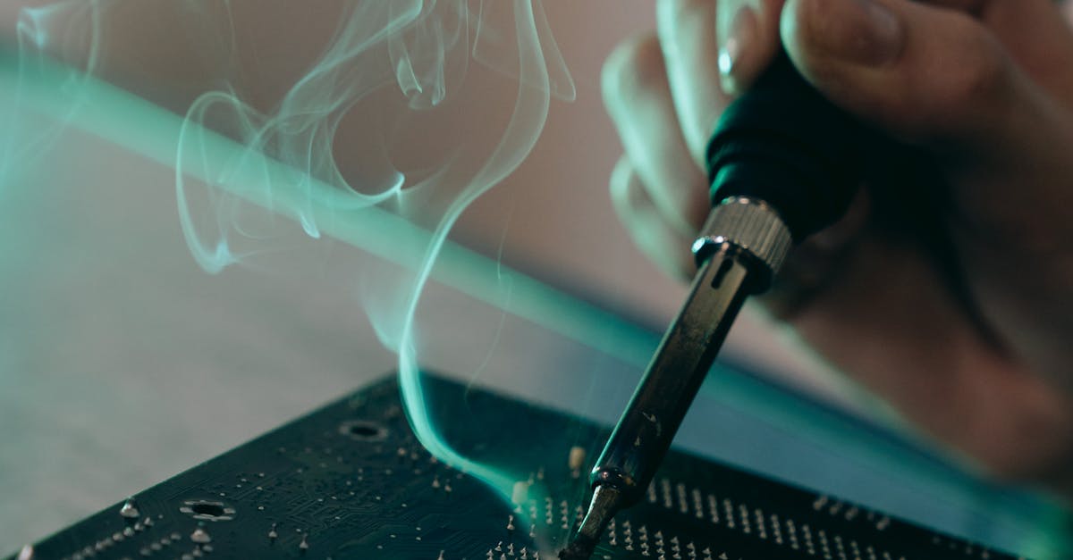
Once all the necessary components have been placed on the board, a reflow oven is used to melt the solder that joins them together. This stage requires precise control over temperature and atmosphere to ensure a smooth soldering process.
After soldering, the PCB undergoes various tests including visual inspection for any signs of defects or damage, electrical testing to verify component functionality, and environmental testing to assess the board’s durability in different conditions.
Finally, the completed electronic boards are packaged and shipped out to manufacturers where they’re integrated into their respective devices. Throughout this entire process, quality control measures are taken at every stage to ensure that the final product meets the required standards of performance and reliability.
The process of making electronic boards is a complex one that involves multiple stages each requiring precise execution. Despite these complexities, manufacturing facilities have developed efficient processes that enable them to produce high-quality PCBs in large quantities while maintaining cost-effectiveness.
Photos provided by Pexels
